Get Quote
730 people are quoting
X

Large-sized Silicon Nitride AMB Substrate

11 month ago
49 0
Product details

Silicon Nitride Ceramic AMB Copper-clad Substrate

Puwei's Silicon Nitride Ceramic AMB Copper-clad Substrate represents the pinnacle of advanced ceramic substrate technology for demanding power devices and high-reliability electronic packaging. Utilizing Active Metal Brazing (AMB) technology, we bond high-conductivity copper to premium silicon nitride (Si₃N₄) ceramic, delivering exceptional thermal, mechanical, and electrical performance for next-generation SiC and GaN applications. This substrate is engineered as the ultimate solution for high-power microelectronic components requiring unmatched reliability.
Core Performance Advantages

  • Exceptional Mechanical Strength: >800 MPa flexural strength, 3-5x stronger than alumina.
  • Superior Thermal Shock Resistance: Outperforms Al₂O₃ and AlN in rapid temperature cycling.
  • Optimal CTE Matching: 3.2 ppm/°C closely matches SiC semiconductors (3.7 ppm/°C).
  • High Reliability Bonding: AMB creates stronger metallurgical bonds than traditional DBC methods.
  • Robust Thermal Performance: 80-90 W/m·K thermal conductivity with excellent stability.
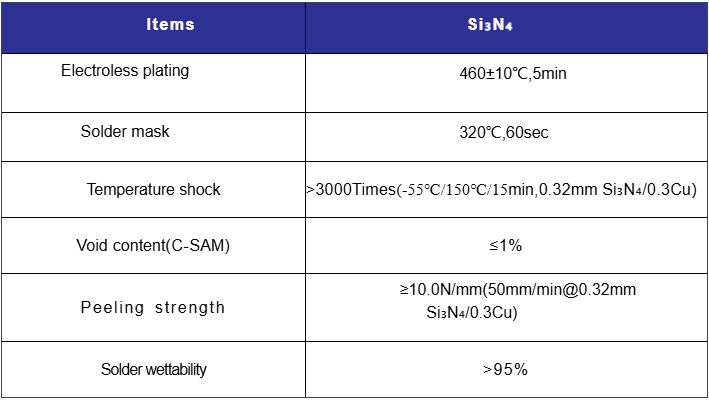
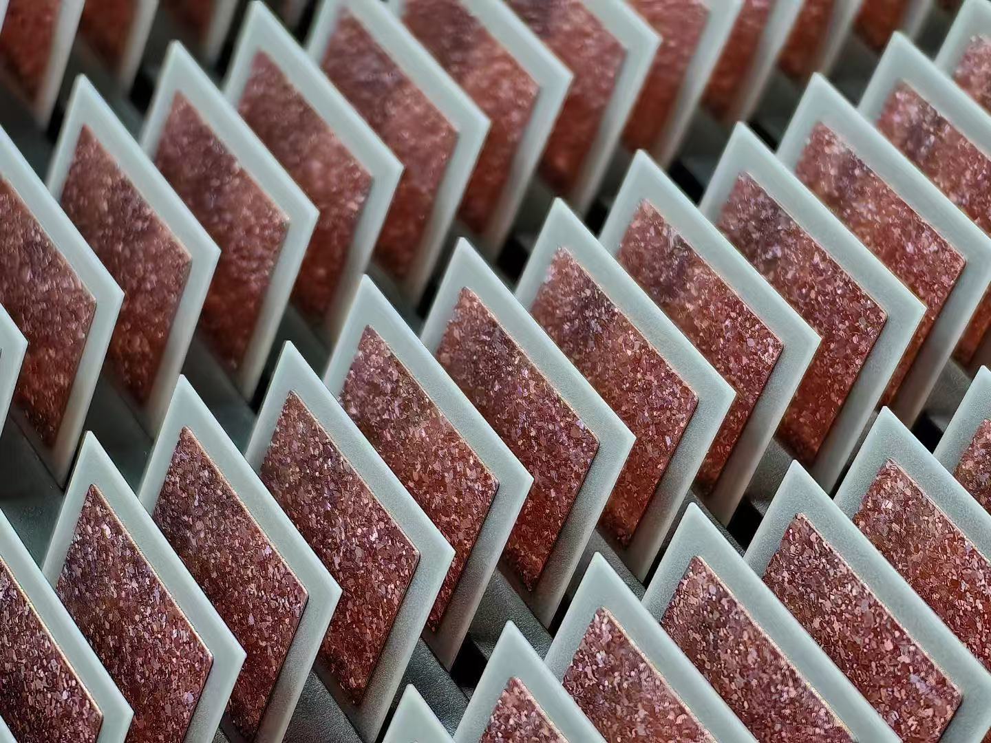
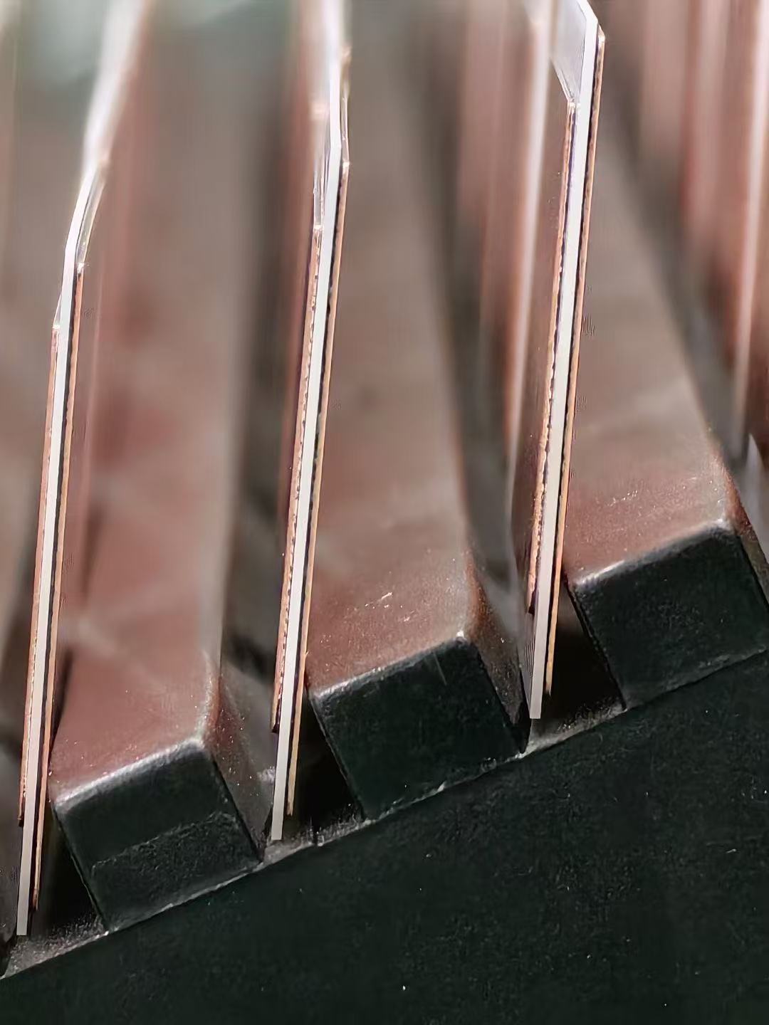
High-performance AMB Silicon Nitride Ceramic Substrate for SiC power applications Detailed view of Silicon Nitride AMB substrate with precision copper patterning Technical properties and performance comparison of Si3N4 AMB substrates

Technical Specifications

Our Si₃N₄ AMB substrates are characterized by precise, high-performance specifications crucial for reliable microelectronics packaging.

Material Properties

Base Material: High-purity Silicon Nitride (Si₃N₄). Cladding Material: Oxygen-free high conductivity copper. Thermal Conductivity: 80-90 W/m·K. Flexural Strength: >800 MPa. CTE: 3.2 ppm/°C. Dielectric Strength: >15 kV/mm. Peel Strength: >80 N/cm.

Dimensions & Tolerances

Ceramic Thickness: 0.25mm-1.0mm standard (0.2mm-2.0mm custom). Copper Thickness: 0.1mm-0.8mm. Maximum Size: 240mm × 280mm. Surface Flatness: <10μm/cm. Thick Copper Capability: Supports up to 0.8mm copper for higher current carrying capacity, ideal for advanced integrated circuit packaging.

Key Features & Technology Advantages

Superior Thermal Shock Resistance

Silicon nitride's unique microstructure prevents crack propagation under rapid temperature changes, making it ideal for harsh environments where alumina ceramic substrates or aluminum nitride ceramics may fail. This is critical for automotive and industrial power devices.

Optimal CTE Matching with Wide Bandgap Semiconductors

The thermal expansion coefficient of 3.2 ppm/°C closely matches Silicon Carbide (SiC) and Gallium Nitride (GaN). This minimizes interfacial thermal stress, extending product lifetime and enhancing reliability in high-power microelectronics applications.

Exceptional Mechanical Strength & Durability

With flexural strength exceeding 800 MPa, it provides 3-5x greater mechanical robustness than standard alumina. This ensures integrity under vibration and mechanical stress in electric vehicle powertrains and heavy industrial equipment.

Advanced AMB Bonding Technology

Active Metal Brazing creates strong chemical bonds between ceramic and copper, offering superior thermal cycling performance and long-term reliability compared to traditional Direct Bonded Copper (DBC) methods. This advanced metallized ceramics process is key for high-reliability electronic packaging.

Primary Application Scenarios

Electric Vehicle Power Electronics

Main inverters, DC-DC converters, and onboard chargers requiring robust performance under vibration, thermal cycling, and high power density. Essential for next-generation SiC-based power devices.

Renewable Energy Systems

Solar inverters and wind power converters demanding long-term reliability and excellent thermal shock resistance in outdoor environments with wide temperature fluctuations.

Industrial Motor Drives & Power Supplies

High-power drives for manufacturing and automation equipment requiring exceptional mechanical strength and thermal cycling performance in harsh industrial settings.

Aerospace, Defense & Rail Transportation

Mission-critical power electronics where the highest levels of reliability, mechanical robustness, and performance under extreme conditions are non-negotiable.

Advanced High-Frequency Modules & RF Power

While optimized for thermal management, its excellent dielectric properties also support demanding RF circuits and microwave applications where reliability is paramount.

Implementation & Design Integration Guide

  1. Application Analysis: Evaluate thermal, mechanical, and reliability requirements against Si₃N₄ AMB advantages.
  2. Thermal Simulation: Utilize our material property data for system-level thermal management design.
  3. Substrate & Circuit Design: Provide layout specifications. We leverage expertise in thick film hybrid microcircuits for optimization.
  4. Prototyping & Validation: Test samples under real operating conditions to verify performance.
  5. Assembly Process Adaptation: Optimize soldering and assembly for silicon nitride's characteristics.
  6. Quality Validation & Scaling: Perform comprehensive testing before scaling to volume production.

Value Proposition for OEMs & Design Engineers

  • Enhanced System Reliability: Drastically reduce field failures in demanding conditions.
  • Extended Product Lifespan: Superior thermal cycling capability ensures longer operational life.
  • Enable Compact, Power-Dense Designs: Higher strength allows for thinner substrates and smaller modules.
  • Improved Total Cost of Ownership (TCO): Reduced failure rates and longer service life offset initial cost.
  • Access to Advanced Expertise: Partner with Puwei for application engineering in microelectronics packaging.

Manufacturing Process & Quality Assurance

Our production ensures the highest purity, density, and dimensional accuracy for critical insulation elements in power modules.

  1. Raw Material Preparation: Selection of high-purity Si₃N₄ powder.
  2. Forming & Sintering: Shaping and high-temperature sintering to achieve optimal microstructure.
  3. Precision Machining: Diamond grinding to exact thickness and flatness.
  4. Surface Activation: Preparation for perfect bonding interface.
  5. Active Metal Brazing (AMB): High-temperature vacuum brazing to create metallurgical bonds.
  6. Patterning & Finishing: Photolithography, etching, and application of protective surface finishes.
  7. Rigorous Quality Inspection: 100% inspection and performance testing of thermal, electrical, and mechanical properties.

Certifications & Compliance

Puwei products meet the highest international standards for quality and reliability.

  • Quality Management: ISO 9001:2015 Certified.
  • Automotive Standard: IATF 16949:2016 Compliance.
  • Material Safety: UL 94 V-0 Flammability Rating.
  • Environmental Compliance: RoHS and REACH directives.

Customization & OEM/ODM Services

We tailor Si₃N₄ AMB substrates to your exact requirements for advanced electronic packaging.

  • Dimensions & Geometry: Custom sizes up to 240mm × 280mm, complex shapes, and contours.
  • Layer Thickness: Precise control of ceramic (0.2-2.0mm) and copper (0.1-0.8mm) thickness.
  • Circuit Patterning: Complex designs with fine features for optimized current paths.
  • Surface Finishes: Ni/Au, Ni/Pd, Ag, or Sn plating for enhanced solderability and protection.
  • Material & Process Optimization: Tailored solutions for specific operational environments and performance targets.
Contact Now

If you are interested in the product, contact 2bvideo.com for more information for more information

To:
Shaanxi Puwei Electronic Technology Co., Ltd
Message:
Submit
Disclaimer:

The information of 2bvideo.com limited shown above is provided by the user or collected on the network. Video 2B does not guarantee the authenticity,accuracy and legitimacy of 2bvideo.com limited information. Video 2B does not involve legal relationships and disputes between users arising from transactions other than secured transactions on this website. Disputes shall be settled by you through negotiation. If you are the person in charge or relevant employee of this enterprise, if you find that the enterprise information is incorrect or want to manage thiscompany, please contact us jacklee1558@gmail.com, after you claim the enterprise, you can obtain management permission, publish supplyand demand information, bring consulting orders, and remove page advertisements.

Audited supplier
2 year
Address: Xian, China


Main Product: Alumina Ceramic Substrates, Aluminum Nitride Substrates, Metallized Ceramics, AlN Ceramics Disc, DPC Substrate , DBC Ceramic Substrate

Disclaimer:
The information of 2bvideo.com limited shown above is provided by the user or collected on the network. Video 2B does not guarantee the authenticity,accuracy and legitimacy of 2bvideo.com limited information. Video 2B does not involve legal relationships and disputes between users arising from transactions other than secured transactions on this website. Disputes shall be settled by you through negotiation. If you are the person in charge or relevant employee of this enterprise, if you find that the enterprise information is incorrect or want to manage thiscompany, please contact us jacklee1558@gmail.com, after you claim the enterprise, you can obtain management permission, publish supplyand demand information, bring consulting orders, and remove page advertisements.
Content Us